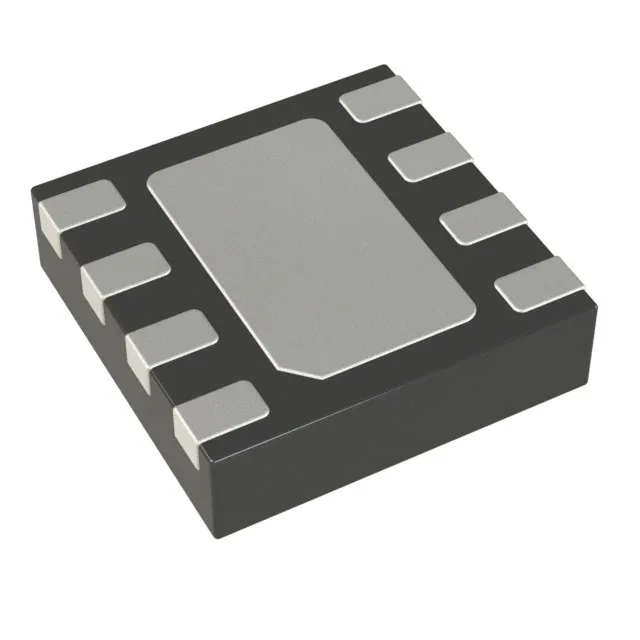
Analog Devices ADP7183ACPZN2.0-R7 — Microcontrollers & Processors (MCU / MPU / DSP)

ADP7183ACPZN2.0-R7 Negative LDO, -2V Fixed, 300mA, 8-LFCSP

MPNADP7183ACPZN2.0-R7
End of Life

Analog Devices ADP7183ACPZN2.0-R7 negative linear regulator, fixed -2V output, 300mA, 85dB PSRR at 1kHz, 8-UFDFN exposed pad CSP, tape and reel.

$5.25Ref. price · indicative, final on quote
Packaging8-UFDFN Exposed Pad, CSP
StockContact for availability
Lead timeIn Stock wk
MOQ1 pcs
  • 100% new & originalTraceable channels only — no refurbs, no pulls, no remarked parts.
  • Date & lot codes on quoteStated per line before you commit; label photos on request.
  • MSL-compliant ESD packingMoisture-sealed bags with indicator cards; reels photo-verified.
  • PayPal buyer protectionPay by T/T, PayPal or Payoneer — card payments covered end to end.

Specifications

ADP7183ACPZN2.0-R7 Technical Specifications
ParameterValue
Output typeFixed
Mounting typeSurface Mount
Voltage - input-5.5V
Voltage dropout0.22V @ 300mA
Voltage - output (Min (Fixed))-2V
Current - output300mA
Current - supply7 mA
Current - quiescent900 µA
Operating temperature-40°C ~ 125°C (TJ)
PSRR85dB ~ 40dB (1kHz ~ 1MHz)
PackageTape & Reel (TR); Cut Tape (CT)
Case8-UFDFN Exposed Pad, CSP
Control featuresEnable
Protection featuresCurrent Limit, Thermal Overload
Number of regulators1
Output configurationNegative

Product details

Negative rail generator for noise-sensitive analog front-ends

The ADP7183ACPZN2.0-R7 is a single-output negative linear regulator from Analog Devices, delivering a fixed -2 V output at up to 300 mA from a maximum -5.5 V input rail. Its 85 dB PSRR at 1 kHz, rolling off to 40 dB at 1 MHz, means it cleans up switching-noise ripple from a negative buck-boost or charge pump before it reaches the analog load — a key spec for precision ADC and op-amp supply rails where power-supply rejection at the load is already tight.

Dropout voltage and headroom budgeting

Maximum dropout is 220 mV at the full 300 mA load — the input rail must stay at least 220 mV more negative than -2 V across the load range, or the output falls out of regulation. Quiescent current is 900 µA typical, rising to 7 mA max under supply — the 900 µA floor is the regulator's own draw from the input rail regardless of load, which matters for battery-powered gear where the negative rail runs continuously.

The Enable control pin allows the regulator to be shut down externally, pulling the quiescent current to near zero when the negative rail is not needed — useful for sequenced power-up in multi-rail systems.

Sourcing and compliance status

ROHS3 compliant per the manufacturer's declaration, with no exemptions for lead or restricted substances under the current EU directive. Supplied in tape-and-reel packaging (7-inch reel, 3000 pieces per reel) or cut-tape for prototype quantities — the -R7 suffix identifies the reel quantity variant.

Frequently asked questions

Will ADP7183ACPZN2.0-R7 drop into a board designed for ADP7183ACPZN2.5-R7?

Yes — the ADP7183ACPZN2.5-R7 uses the same die, package (8-LFCSP 2x2 mm), pinout, and external component requirements. The only difference is the fixed output voltage: -2.0 V versus -2.5 V. A BOM-line swap from one to the other requires no PCB respin, only a change in the output voltage the downstream load expects.

What is the PSRR of ADP7183ACPZN2.0-R7 across frequency?

The ADP7183ACPZN2.0-R7 delivers 85 dB of power-supply rejection at 1 kHz, decreasing to 40 dB at 1 MHz. This roll-off is typical for a linear regulator — the control loop gain drops above the unity-gain crossover. For switching-noise frequencies above 1 MHz, additional filtering (a ferrite bead or LC stage) ahead of the regulator improves the effective rejection.