Noise-sensitive rail regulator with 40V input tolerance
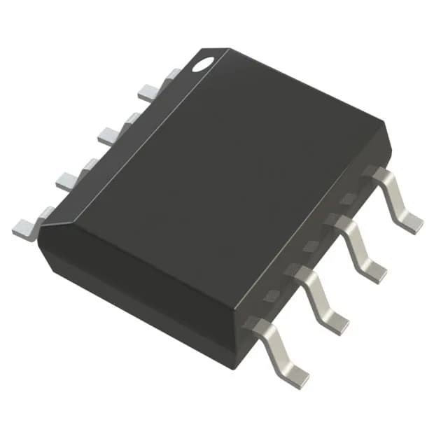
The Analog Devices ADP7142ARDZ-5.0-R7 is a fixed 5V output low-dropout linear regulator rated for 200 mA continuous output. The 88 dB PSRR at 10 kHz is the headline spec here — this part is built for analog and RF supply rails where switching-regulator ripple would couple into the signal path. Dropout voltage maxes at 0.42 V at the full 200 mA load, so a 5.5 V input holds regulation through a cold-crank dip. Quiescent current sits at 140 µA, low enough for always-on blocks in battery-backed systems. The exposed-pad SOIC-8 package helps pull heat to the PCB copper; the thermal pad wants a via stitch under the pad to keep junction temperature in check above 100 mA continuous.
PSRR across frequency — what it buys you
The PSRR curve starts at 88 dB at 10 kHz and rolls off to 50 dB at 1 MHz. That 88 dB at 10 kHz means a 100 mVpp ripple on the input — typical from a 200 kHz buck converter — gets attenuated to about 400 µVpp at the output. For a 5 V rail feeding a 24-bit ADC or a VCO, that keeps the noise floor out of the conversion band. The roll-off above 100 kHz is normal for a linear regulator; if you need rejection at 2–3 MHz, pair this with a ferrite bead and 1 µF ceramic on the output. The 50 dB at 1 MHz still gives 316× attenuation, enough to clean up most switching noise from a 1 MHz converter.
Dropout and headroom planning
Maximum dropout is 0.42 V at 200 mA. For a 5 V output, that means the input must stay above 5.42 V worst-case to maintain regulation. In practice, a 6 V or 9 V rail gives comfortable margin. If the input drops to 5.5 V during a battery sag, the output still holds at 5 V as long as the load stays under 200 mA. The enable and soft-start pins let you sequence the rail — useful when powering a sensor that needs a clean ramp to avoid latch-up on the downstream IC.
Temperature range and environment
The 125°C ceiling covers the hot spots near a power stage or in a sealed enclosure. The exposed pad is the primary heat path — without a good thermal connection to the PCB copper, the junction temperature will exceed the 125°C limit at high input-to-output differential and 200 mA load.