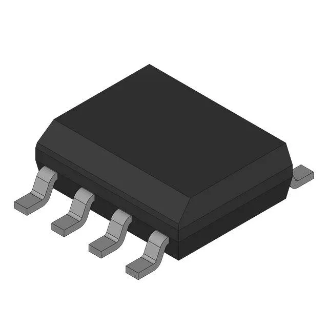
Analog Devices ADP3412JR

ADP3412JR Dual MOSFET Driver, Half-Bridge, 20ns, 8-SOIC

MPNADP3412JR
End of Life

Analog Devices ADP3412JR, dual N-channel MOSFET driver, half-bridge, non-inverting, synchronous, 20ns rise/fall, 4.15V to 7.5V supply, 30V bootstrap max, 0°C to 125°C, 8-SOIC.

$0.87Ref. price · indicative, final on quote
Packaging8-SOIC (0.154", 3.90mm Width)
StockContact for availability
MOQ1 pcs
  • 100% new & originalTraceable channels only — no refurbs, no pulls, no remarked parts.
  • Date & lot codes on quoteStated per line before you commit; label photos on request.
  • MSL-compliant ESD packingMoisture-sealed bags with indicator cards; reels photo-verified.
  • PayPal buyer protectionPay by T/T, PayPal or Payoneer — card payments covered end to end.

Specifications

ADP3412JR Technical Specifications
ParameterValue
Gate typeN-Channel MOSFET
Input typeNon-Inverting
Channel typeSynchronous
Mounting typeSurface Mount
Voltage4.15V ~ 7.5V
Logic voltage - VIL, VIH0.8V, 2V
High side voltage - max (Bootstrap)30 V
Operating temperature0°C ~ 125°C (TJ)
PackageBulk
Case8-SOIC (0.154\", 3.90mm Width)
Number of drivers2
Driven configurationHalf-Bridge
Rise (Fall time)20ns, 20ns

Product details

Half-bridge driver for a synchronous buck rail

The ADP3412JR is a dual N-channel MOSFET driver from Analog Devices, configured as a half-bridge with synchronous drive for the high-side and low-side FETs. It is the glue between a PWM controller and the power stage in a synchronous buck converter, typically found on voltage regulator modules for processor cores, telecom line cards, and base station power supplies.

20 ns edges — dead-time and switching loss budget

The 20 ns typical rise and fall time sets the transition window where both FETs are off. A controller with adaptive dead-time can use this edge rate to minimise body-diode conduction loss without risking shoot-through. The 20 ns spec is fast enough for switching frequencies up to about 500 kHz before the dead-time eats into the duty-cycle range. Supply range of 4.15 V to 7.5 V means this driver runs from a 5 V or 7 V rail, not the 12 V bus common on older half-bridge drivers. The gate drive voltage is therefore limited to the supply rail minus the bootstrap diode drop — about 4.5 V to 7 V at the high-side gate. That is enough to fully enhance a logic-level N-channel MOSFET with a Vgs(th) below 2.5 V. The bootstrap pin is rated to 30 V maximum, which caps the input voltage of the buck converter at about 24 V nominal with margin. A 48 V input bus would exceed the bootstrap rating and damage the driver.

The 125°C upper limit is typical for a junction-temperature-rated driver; the actual case temperature will be lower depending on the thermal impedance of the 8-SOIC footprint.

The 8-SOIC package is a common, low-cost footprint that rework techs can replace with hot air — no preheater needed.

Frequently asked questions

Can ADP3412JR be used with 3.3V logic?

The logic input thresholds are specified at 0.8 V for VIL and 2 V for VIH. A 3.3 V logic output with a 2 V VIH threshold will drive the input reliably, provided the driver's supply voltage is within the 4.15 V to 7.5 V range. The 3.3 V PWM controller output is compatible.

What is the closest functional second-source to ADP3412JR?

The ADP3415LRM-REEL7 is a functional peer — same dual N-channel half-bridge topology, same 20 ns rise/fall time, same non-inverting input. The ADP3415 is specified for 0°C to 100°C ambient, not 125°C junction, and its supply voltage is 7 V nominal. Check the temperature grade and supply rail against your design before substituting.