Analog Devices ADF4002BRUZ — Clock & Timing ICs

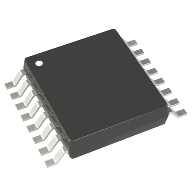
ADF4002BRUZ PLL Clock Synthesizer – 400 MHz, 16-TSSOP

MPNADF4002BRUZ
End of Life

Analog Devices ADF4002BRUZ, Clock/Frequency Synthesizer (RF), Phase Detector, PLL Yes with Bypass, 400 MHz max, 2.7V–3.3V supply, -40°C to 85°C, 16-TSSOP, Tube, ROHS3

$5.78Ref. price · indicative, final on quote
Packaging16-TSSOP (0.173", 4.40mm Width)
StockContact for availability
MOQ1 pcs
  • 100% new & originalTraceable channels only — no refurbs, no pulls, no remarked parts.
  • Date & lot codes on quoteStated per line before you commit; label photos on request.
  • MSL-compliant ESD packingMoisture-sealed bags with indicator cards; reels photo-verified.
  • PayPal buyer protectionPay by T/T, PayPal or Payoneer — card payments covered end to end.

Specifications

ADF4002BRUZ Technical Specifications
ParameterValue
TypeClock/Frequency Synthesizer (RF), Phase Detector
Mounting typeSurface Mount
Voltage2.7V ~ 3.3V
Frequency400MHz
Operating temperature-40°C ~ 85°C
PLLYes with Bypass
InputCMOS, TTL
OutputClock
PackageTube
Case16-TSSOP (0.173\", 4.40mm Width)
Divider (Multiplier)Yes/No
Number of circuits1
Ratio - Input:Output2:1
Differential - Input:OutputYes/No

Product details

400 MHz PLL with bypass – what it does for your RF loop

The ADF4002BRUZ is a PLL clock/frequency synthesizer with a phase detector and a bypass mode, targeting RF synthesizer and clock clean-up applications where the reference runs up to 400 MHz. The integrated PLL includes a charge pump and a programmable divider, but the bypass path lets you feed the reference clock straight through when the loop is not needed — useful for test modes or redundant clock paths.

Supply and temperature – fits 3.3V industrial designs

Runs on a single 2.7V to 3.3V rail, matching the common 3.3V supply used in base station and wireless infrastructure boards. Inputs accept CMOS or TTL levels, so you can interface directly with a crystal oscillator or a 3.3V FPGA output without external level shifting. The single-ended clock output is also CMOS/TTL-compatible.

Package and footprint – 16-TSSOP layout note

Housed in a 16-TSSOP package with 0.65 mm lead pitch, the ADF4002BRUZ fits a standard 4.40 mm-wide body. The supplier device package is also 16-TSSOP; no exposed pad, so a 2-layer board with a solid ground plane under the device is adequate for thermal management at the rated supply current.

Frequently asked questions

Is the ADF4002BRUZ obsolete or still active?

Active. No end-of-life or last-time-buy notice has been issued. The part is current production from Analog Devices.

What is the maximum frequency the ADF4002BRUZ can handle?

The maximum input/output frequency is 400 MHz. This is the upper limit for the reference input and the VCO output through the PLL path.