400 MHz PLL with bypass — what it buys the timing tree
The ADF4002BCPZ is a phase-locked loop with a dedicated bypass path, rated to 400 MHz maximum input frequency. When bypass is engaged, the part collapses to a simple phase detector — useful for system-level test modes or for reusing the same BOM position across a multi-rate product family where one variant needs a clean clock buffer and another needs closed-loop synthesis. The supply range of 2.7V to 3.3V aligns with common 3.3V and 2.5V logic rails; the 2:1 input-to-output ratio means two reference inputs can be muxed into one output path, saving an external RF switch in multi-reference designs.
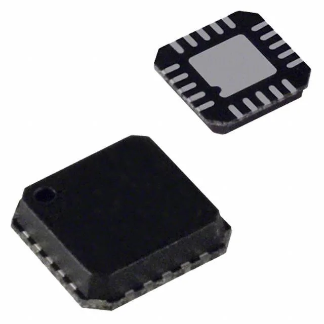
The 20-LFCSP (4x4 mm) exposed-paddle package requires a thermal-via array under the pad — the layout engineer must reserve that area early; the paddle also serves as the primary ground return for the PLL charge pump.