Analog Devices ADF4001BCPZ — Clock & Timing ICs

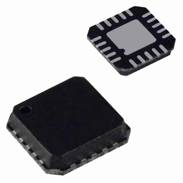
ADF4001BCPZ Clock Generator IC – 200 MHz PLL, LFCSP-20

MPNADF4001BCPZ
End of Life

Analog Devices ADF4001BCPZ, Clock Generator (RF), PLL Yes, 200 MHz max, 2.7 V ~ 5.5 V supply, -40°C ~ 85°C, 20-LFCSP (4x4) package, Tray.

$6.1Ref. price · indicative, final on quote
Packaging20-WFQFN Exposed Pad, CSP
StockContact for availability
MOQ1 pcs
  • 100% new & originalTraceable channels only — no refurbs, no pulls, no remarked parts.
  • Date & lot codes on quoteStated per line before you commit; label photos on request.
  • MSL-compliant ESD packingMoisture-sealed bags with indicator cards; reels photo-verified.
  • PayPal buyer protectionPay by T/T, PayPal or Payoneer — card payments covered end to end.

Specifications

ADF4001BCPZ Technical Specifications
ParameterValue
TypeClock Generator (RF)
Mounting typeSurface Mount
Voltage2.7V ~ 5.5V
Frequency200MHz
Operating temperature-40°C ~ 85°C
PLLYes
InputCMOS, TTL
OutputClock
PackageTray
Case20-WFQFN Exposed Pad, CSP
Divider (Multiplier)Yes/No
Number of circuits1
Ratio - Input:Output2:1
Differential - Input:OutputYes/No

Product details

200 MHz PLL clock generator in a 4x4 mm LFCSP

The ADF4001BCPZ is a phase-locked loop (PLL) clock generator from Analog Devices, built for RF synthesis applications where a clean, stable clock is needed from a lower-frequency reference. It accepts CMOS or TTL inputs and delivers a single clock output at frequencies up to 200 MHz. The 2:1 input-to-output ratio means the chip can select between two reference sources or divide the PLL output internally — useful when the system has a primary and a backup oscillator.

The wide supply range lets the ADF4001BCPZ run directly off a 3.3 V or 5 V rail without a local LDO. That saves a regulator and a couple of bypass caps on the BOM, but the trade-off is that the PLL charge-pump current and loop-filter component values need to be recalculated if the supply voltage changes between designs. Industrial temperature grade qualifies the part for outdoor and factory-floor environments where the ambient can hit 85 °C — common in telecom base stations, motor drives, and instrumentation.

Active production — no obsolescence risk

It ships in a tray — the 20-LFCSP (4x4) package is a standard 4 mm × 4 mm QFN-style footprint with an exposed pad that must be soldered to a thermal land on the PCB for rated heat dissipation.

Package and footprint notes for layout

The 20-WFQFN exposed-pad package has a 0.50 mm pitch. The centre pad is the primary thermal path — the PCB land pattern should include a grid of thermal vias to a ground plane, and the pad must be connected to the ground plane (or the appropriate supply rail) per the datasheet recommendation. Differential input and output capability means the reference and the PLL output can be routed as differential pairs, which helps reject common-mode noise on long board traces or through connectors.

Frequently asked questions

What is the maximum frequency of the ADF4001BCPZ?

The maximum output frequency is 200 MHz. This is the upper limit of the PLL's VCO range; the actual loop bandwidth will be lower depending on the reference frequency and the loop-filter design.

Does the ADF4001BCPZ have a direct replacement or equivalent?

The ADF4001BRUZ-R7 and ADF4001BRUZ are functionally identical PLL clock generators from the same ADF4001 family, but they come in a TSSOP-16 package (not LFCSP). The ADF4007BCPZ is a higher-frequency sibling (7.5 GHz) in the same LFCSP footprint, but it is a clock/frequency synthesizer rather than a pure clock generator. None of these are drop-in replacements — the package and pinout differ.

What supply voltage does the ADF4001BCPZ need?

The charge-pump current and loop-filter component values depend on the actual supply voltage used.