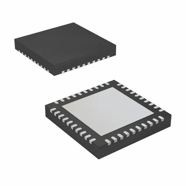
Clock distribution at 4.8 GHz — what the fanout ratio means for your BOM
The ADCLK954BCPZ is a SiGe fanout buffer that accepts one of two selectable clock inputs and delivers twelve LVPECL copies at up to 4.8 GHz. That 2:12 ratio means a single device can feed a dozen high-speed loads — ADCs, FPGAs, or SerDes — without cascading multiple buffers, saving board area and reducing additive jitter from extra stages. Input compatibility spans CMOS, LVDS, and LVPECL levels, so the same part can interface with a crystal oscillator, a PLL output, or a backplane clock without external level shifters. The fully differential signal path (input and output) preserves common-mode rejection and keeps the clock clean through the distribution tree.
Supply rail and temperature — staying inside the operating window
The supply range is 2.97 V to 3.63 V, a tight 3.3 V nominal window. Plan for a low-noise LDO or a clean switching regulator with ripple below 10 mV to keep the clock jitter floor low.
Active production — no EOL risk for current designs
The part is in ongoing production at Analog Devices, and the tray package is the standard delivery format for volume assembly — no reel premium. ROHS3 compliant, so it passes EU material restrictions without an exemption. The 40-LFCSP package is lead-free compatible with standard Pb-free reflow profiles (260°C peak).