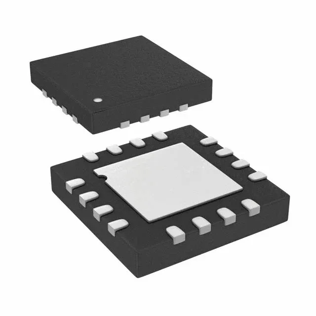
Analog Devices ADCLK914BCPZ-R7 — Clock & Timing ICs

ADCLK914BCPZ-R7 Clock Buffer 7.5 GHz SiGe – Analog Devices

MPNADCLK914BCPZ-R7
End of Life

Analog Devices ADCLK914BCPZ-R7, SiGe series, Clock & Timing IC, Buffer/Driver, Data, 1 circuit, 1:1 ratio, 7.5 GHz max, 2.97V–3.63V supply, -40°C to 125°C, 16-LFCSP-VQ (3x3 mm).

$19.09Ref. price · indicative, final on quote
Packaging16-VFQFN Exposed Pad, CSP
StockContact for availability
MOQ1 pcs
  • 100% new & originalTraceable channels only — no refurbs, no pulls, no remarked parts.
  • Date & lot codes on quoteStated per line before you commit; label photos on request.
  • MSL-compliant ESD packingMoisture-sealed bags with indicator cards; reels photo-verified.
  • PayPal buyer protectionPay by T/T, PayPal or Payoneer — card payments covered end to end.

Specifications

ADCLK914BCPZ-R7 Technical Specifications
ParameterValue
TypeBuffer/Driver, Data
SeriesSiGe
Mounting typeSurface Mount
Voltage2.97V ~ 3.63V
Frequency7.5 GHz
Operating temperature-40°C ~ 125°C
InputCML, CMOS, LVDS, LVPECL, LVTTL
OutputHVDS
PackageTape & Reel (TR); Cut Tape (CT)
Case16-VFQFN Exposed Pad, CSP
Number of circuits1
Ratio - Input:Output1:1
Differential - Input:OutputYes/Yes

Product details

7.5 GHz clock distribution in a 3x3 mm footprint

The ADCLK914BCPZ-R7 is a 1:1 clock buffer/driver from Analog Devices' SiGe series, rated for a maximum frequency of 7.5 GHz. That speed ceiling makes it a fit for distributing high-frequency reference clocks to ADCs, DACs, and SERDES transceivers where edge jitter and deterministic skew matter more than fan-out count. It accepts a wide range of input signal types — CML, CMOS, LVDS, LVPECL, and LVTTL — and outputs HVDS. That means you can feed it from nearly any standard clock source without a separate level translator, which simplifies the BOM and saves board area. The supply range is 2.97V to 3.63V, so it runs on a single 3.3V rail with margin for ripple. The 1:1 input-to-output ratio means it is a pure buffer — no division, no multiplication — just clean regeneration of the incoming clock.

Temperature grade and package constraints

The 16-LFCSP-VQ (3x3 mm) package has an exposed pad that must be soldered to a thermal land on the PCB; the datasheet's recommended footprint includes a via array under the pad to pull heat into the ground plane. The exposed pad is also the ground return for the high-speed signal path — a poor thermal connection here degrades both thermal impedance and signal integrity. For a rework tech: this is a QFN-style package; hot-air removal is routine, but the pad under the centre can be stubborn if the board has a thick ground plane. Pre-bake at 125°C for 8 hours if the parts have been exposed to humidity above MSL level 3.

Sourcing and lifecycle status

It is ROHS3 compliant and available in tape-and-reel (TR) or cut-tape (CT) packaging. For volume BOM planning, this is a single-source part from ADI — no direct second-source with the same 7.5 GHz rating and multi-protocol input is listed. Pricing and lead time are confirmed at RFQ; the part is sourced to order against your BOM quantity.

Frequently asked questions

What input signal types does the ADCLK914BCPZ-R7 accept?

It accepts CML, CMOS, LVDS, LVPECL, and LVTTL inputs. The output is HVDS. This wide input compatibility means you can drive it from most standard clock sources without extra level-shifting components.