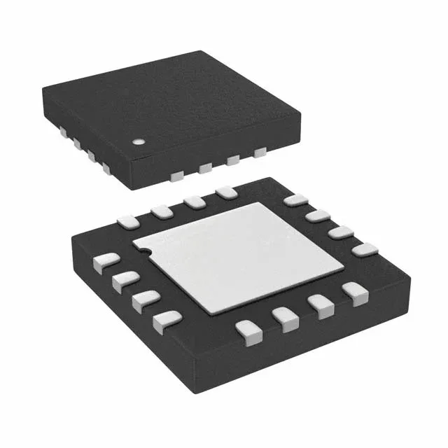
7.5 GHz buffer — clock distribution for high-speed converters
The ADCLK907BCPZ-WP: This is a dual-channel clock buffer with a 1:1 fanout, rated for a maximum frequency of 7.5 GHz. The differential input and output preserve signal integrity over long PCB traces or coax, making it a natural fit for driving the clock inputs of high-speed ADCs, DACs, or FPGA transceivers where jitter budget is tight. Outputs are configurable as ECL, NECL, or PECL, which means the same part can interface with 2.5V or 3.3V logic families by adjusting the supply voltage — no level translator needed.
Supply voltage and temperature — board-level fit
The supply range spans 2.375V to 3.63V, covering standard 2.5V and 3.3V rails. The 16-LFCSP-VQ (3x3) package has an exposed pad that must be soldered to a thermal land on the PCB. Check the MSL rating before reflow — the small pad pitch demands a controlled profile to avoid solder bridging.
