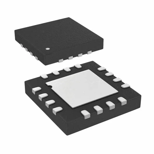
Analog Devices ADCLK905BCPZ-R2 — Clock & Timing ICs

ADCLK905BCPZ-R2 Clock Buffer 7.5 GHz SiGe 16-LFCSP

MPNADCLK905BCPZ-R2
End of Life

Analog Devices SiGe series, ADCLK905BCPZ-R2, Clock Buffer/Driver, Data, 1:1 fanout, 7.5 GHz max frequency, differential I/O, ECL/NECL/PECL outputs, 16-VFQFN Exposed Pad (LFCSP), -40°C to 125°C.

$14.49Ref. price · indicative, final on quote
Packaging16-VFQFN Exposed Pad, CSP
StockContact for availability
MOQ1 pcs
  • 100% new & originalTraceable channels only — no refurbs, no pulls, no remarked parts.
  • Date & lot codes on quoteStated per line before you commit; label photos on request.
  • MSL-compliant ESD packingMoisture-sealed bags with indicator cards; reels photo-verified.
  • PayPal buyer protectionPay by T/T, PayPal or Payoneer — card payments covered end to end.

Specifications

ADCLK905BCPZ-R2 Technical Specifications
ParameterValue
TypeBuffer/Driver, Data
SeriesSiGe
Mounting typeSurface Mount
Voltage2.375V ~ 3.63V
Frequency7.5 GHz
Operating temperature-40°C ~ 125°C
InputClock
OutputECL, NECL, PECL
PackageTape & Reel (TR); Cut Tape (CT)
Case16-VFQFN Exposed Pad, CSP
Number of circuits1
Ratio - Input:Output1:1
Differential - Input:OutputYes/Yes

Product details

The ADCLK905BCPZ-R2 is a single-channel clock buffer from Analog Devices' SiGe family, designed to distribute high-frequency clock or data signals with minimal additive jitter. It accepts a differential clock input and delivers a differential output at ECL, NECL, or PECL levels — the output logic family is set by the supply voltage and termination scheme. With a maximum frequency of 7.5 GHz, this part targets RF test equipment, high-speed ADC clock distribution, optical transceiver modules, and broadband data buffering where signal integrity at multi-GHz rates is non-negotiable.

Supply range and temperature grade — design margin

The supply voltage spans 2.375 V to 3.63 V, covering both 2.5 V and 3.3 V nominal rails. This eliminates the need for a dedicated regulator when the board already carries one of those voltages — a practical BOM simplification.

Package and footprint — 16-LFCSP with exposed pad

Housed in a 16-lead LFCSP (3 mm × 3 mm) with an exposed pad, the package requires a thermal via array under the pad to conduct heat to the PCB ground plane. The small footprint saves board area in dense RF layouts.

Active production — no obsolescence pressure

There is no end-of-life notice or last-time-buy deadline — it remains a supported, orderable part for new and existing designs.

Frequently asked questions

Is ADCLK905BCPZ-R2 available in tape and reel?

Yes, the -R2 suffix indicates tape-and-reel packaging (250 pieces per reel). It is also available in cut tape for smaller quantities.

What is the closest functional second-source to ADCLK905BCPZ-R2?

The ADCLK905BCPZ-R7 is the same die in a different reel quantity (7-inch reel vs 13-inch). The ADCLK907BCPZ-R2 is a dual-channel version (2 circuits, 1:1 fanout per channel) in the same package — a drop-in replacement if you need two buffers on one footprint.