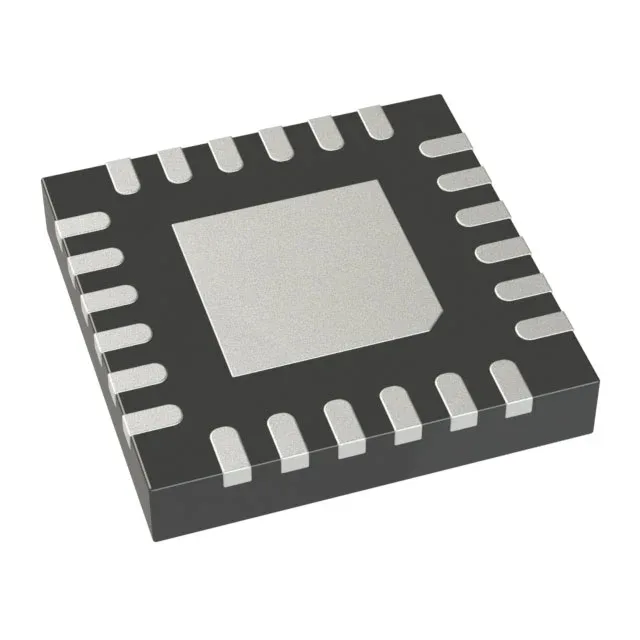
1.2 GHz fanout buffer for high-speed clock trees
The ADCLK846BCPZ is a 1:6 fanout buffer rated for a maximum frequency of 1.2 GHz. That 1.2 GHz ceiling means it can distribute a 1 GHz ADC sampling clock or a 156.25 MHz Ethernet reference with plenty of margin — the buffer itself is rarely the bottleneck. It accepts CML, CMOS, HSTL, LVDS, and LVPECL inputs and outputs CMOS or LVDS. The input flexibility is the key feature here: you can feed it from a crystal oscillator, a PLL synthesizer, or a serializer output without adding a level-shifter.
The supply range is 1.71V to 1.89V, which maps to a nominal 1.8V rail. The 180 mV tolerance means the rail needs a low-noise LDO — a switcher with 50 mV ripple will push the output jitter above the buffer's own additive jitter floor.
The tray package is the standard delivery form for volume assembly. For smaller quantities, the ADCLK846BCPZ-REEL7 variant ships in tape and reel — electrically identical, same 24-LFCSP footprint.
Input and output signal compatibility
Differential input and output paths are supported, which preserves signal integrity over longer PCB traces. The single-circuit design means one buffer IC handles one clock input and fans it to six outputs — no daisy-chaining needed for a six-way split. Surface-mount mounting in the 24-WFQFN exposed pad package requires a solder stencil aperture covering at least 50% of the pad area to avoid voids under the thermal slug.