Why the 170 V/µs slew rate matters for your signal chain
The ADA4891-3WARUZ-R7 is a triple CMOS op-amp from Analog Devices built for applications where settling time and large-signal bandwidth decide the output fidelity. Its 170 V/µs slew rate means a 2 V step settles in roughly 12 ns — fast enough to buffer video signals, drive the input of a high-speed ADC, or handle the transient edges in a multiplexed data-acquisition front end without introducing slew-induced distortion. The 220 MHz -3 dB bandwidth supports small-signal gain stages up to tens of megahertz with clean phase response, making it a fit for active filters, line drivers, and IF amplifier chains.
Supply range and output swing — single-rail operation without the headroom tax
Each of the three channels delivers up to 125 mA of output current, enough to drive a 50 Ω back-terminated cable or a heavy capacitive load in a sample-and-hold stage.
Temperature range and package — industrial and automotive deployment
Supply current and thermal budget — three channels on a single rail
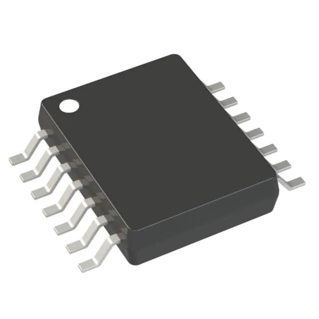
Total quiescent supply current is 4.4 mA per channel, so the three amplifiers together draw about 13.2 mA from the rail at idle. That is modest enough to keep junction temperature rise under 10°C in still air at 25°C ambient, even when driving moderate loads. For continuous high-output-current applications, the 14-TSSOP's thermal resistance (roughly 150°C/W θJA without airflow) means you should check the junction temperature if all three channels are sourcing 50 mA or more simultaneously.
Input bias and offset — CMOS front end for high-impedance sources
The CMOS input stage gives a typical input bias current of 2 pA and an input offset voltage of 2.5 mV. The picoamp-level bias makes the part suitable for buffering high-impedance sensors, photodiodes, and precision integrators where FET-input amplifiers are standard. The 2.5 mV offset is typical for a CMOS op-amp at this speed — adequate for AC-coupled paths and many DC-accurate loops, though a precision amplifier with sub-millivolt offset would be the better choice for microvolt-level measurement chains.