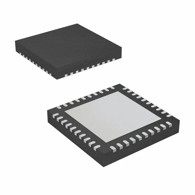
Analog Devices AD9577BCPZ — Clock & Timing ICs

AD9577BCPZ Clock Generator PLL 637.5MHz LVCMOS LVDS LVPECL

MPNAD9577BCPZ
End of Life

Analog Devices AD9577BCPZ, PLL-based clock generator, 637.5 MHz max output, 2:5 input:output ratio, LVCMOS/LVDS/LVPECL outputs, 40-LFCSP-WQ (6x6) package, -40°C to 85°C operation.

$12.73Ref. price · indicative, final on quote
Packaging40-WFQFN Exposed Pad, CSP
StockContact for availability
MOQ1 pcs
  • 100% new & originalTraceable channels only — no refurbs, no pulls, no remarked parts.
  • Date & lot codes on quoteStated per line before you commit; label photos on request.
  • MSL-compliant ESD packingMoisture-sealed bags with indicator cards; reels photo-verified.
  • PayPal buyer protectionPay by T/T, PayPal or Payoneer — card payments covered end to end.

Specifications

AD9577BCPZ Technical Specifications
ParameterValue
Mounting typeSurface Mount
Voltage3V ~ 3.6V
Frequency637.5MHz
Operating temperature-40°C ~ 85°C
PLLYes
InputClock, Crystal
OutputLVCMOS, LVDS, LVPECL
PackageTray
Main purposeEthernet, PCI Express (PCIe), SONET/SDH
Case40-WFQFN Exposed Pad, CSP
Number of circuits1
Ratio - Input:Output2:5
Differential - Input:OutputNo/Yes

Product details

PLL clock generator for multi-rate line cards

The AD9577BCPZ is a dual-PLL clock generator from Analog Devices, purpose-built for Ethernet, PCI Express, and SONET/SDH line cards. It accepts a clock or crystal input and delivers up to five outputs in LVCMOS, LVDS, or LVPECL logic families — covering the three most common backplane clocking standards from a single IC. Maximum output frequency is 637.5 MHz, which covers PCIe Gen3/4 reference clocks and 10GBASE-R line rates. The 2:5 input-to-output ratio means you can distribute one or two reference sources to five downstream PLLs or SerDes without an external fanout buffer.

Output flexibility and supply rail

Each output bank can be independently configured for LVCMOS, LVDS, or LVPECL — a single BOM position handles mixed-logic clock trees. The supply range is 3.0 V to 3.6 V, which aligns with standard 3.3 V backplane rails; no additional LDO is needed for the clock IC. Differential inputs are not supported (the input side is single-ended clock or crystal), but all five outputs can be differential (LVDS or LVPECL). This matters when the reference source is a local oscillator and the fanout targets differential SerDes reference inputs.

Active production and package details

Housed in a 40-lead LFCSP-WQ (6x6 mm) with an exposed pad.

Frequently asked questions

Is AD9577BCPZ compatible with PCIe or Ethernet?

Yes — the main purpose is listed as Ethernet and PCI Express (PCIe), along with SONET/SDH. The 637.5 MHz maximum output covers PCIe Gen3/4 reference clocks and 10GBASE-R line rates.

Does AD9577BCPZ support LVPECL outputs?

Yes. The output types include LVCMOS, LVDS, and LVPECL. Each output can be configured independently for the required logic family.

When sourcing AD9577BCPZ, what is the closest functional alternative?

The tape-and-reel variant AD9577BCPZ-R7 is electrically identical. For a different output count or frequency ceiling, the AD9550BCPZ (1:2 ratio, 810 MHz max) or AD9524BCPZ-REEL7 (2:6 ratio, 1 GHz max, fully differential I/O) are in the same family but have different pinouts — verify the board layout before substituting.