What this clock generator does on your board
The AD9574BCPZ is a PLL-based clock generator from Analog Devices that accepts two clock inputs and delivers seven output banks — each independently configurable as CMOS, HCSL, HSTL, or LVDS. The PLL block includes a bypass path, letting you feed a clean reference straight through when phase noise is more critical than frequency multiplication. Maximum output frequency is 312.5 MHz, which covers the reference clock range for most Gigabit Ethernet PHYs, FPGA transceivers, and ADC/DAC sampling clocks.
Supply rail and output drive — what to plan for
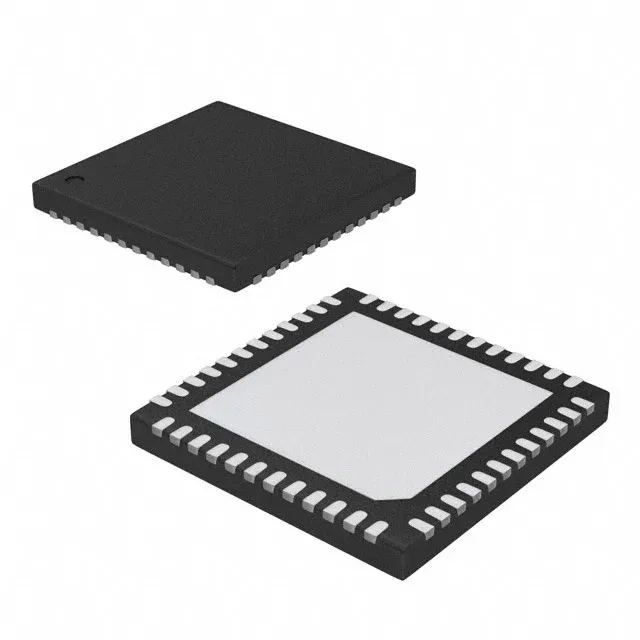
Supply voltage range is 2.97V to 3.63V, nominally a 3.3V rail. No separate 1.8V or 2.5V supply is needed — the output logic levels are generated from the same core supply, so your power-tree design stays simple. The differential input and output capability allows long PCB traces or cable runs with common-mode noise rejection, useful when the clock source is on a separate card. Package is a 48-lead LFCSP with exposed pad, 7x7 mm body.