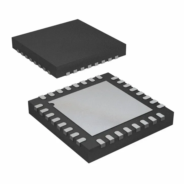
Analog Devices AD9552BCPZ-REEL7 — Clock & Timing ICs

AD9552BCPZ-REEL7 Clock Generator – Analog Devices, 900 MHz

MPNAD9552BCPZ-REEL7
End of Life

Analog Devices AD9552BCPZ-REEL7, Clock Generator, PLL Yes with Bypass, 1 circuit, 2:2 ratio, CMOS/Crystal input, CMOS/LVDS/LVPECL output, 900 MHz max, 32-WFQFN Exposed Pad (5x5 mm), -40°C to 85°C, 3.135V–3.465V supply, Active, ROHS3.

$14.95Ref. price · indicative, final on quote
Packaging32-WFQFN Exposed Pad, CSP
StockContact for availability
MOQ1 pcs
  • 100% new & originalTraceable channels only — no refurbs, no pulls, no remarked parts.
  • Date & lot codes on quoteStated per line before you commit; label photos on request.
  • MSL-compliant ESD packingMoisture-sealed bags with indicator cards; reels photo-verified.
  • PayPal buyer protectionPay by T/T, PayPal or Payoneer — card payments covered end to end.

Specifications

AD9552BCPZ-REEL7 Technical Specifications
ParameterValue
TypeClock Generator
Mounting typeSurface Mount
Voltage3.135V ~ 3.465V
Frequency900MHz
Operating temperature-40°C ~ 85°C
PLLYes with Bypass
InputCMOS, Crystal
OutputCMOS, LVDS, LVPECL
PackageTape & Reel (TR); Cut Tape (CT)
Case32-WFQFN Exposed Pad, CSP
Divider (Multiplier)Yes/No
Number of circuits1
Ratio - Input:Output2:2
Differential - Input:OutputNo/Yes

Product details

PLL clock generator with bypass — what it covers

The AD9552BCPZ-REEL7 is a single-channel clock generator from Analog Devices that accepts either a CMOS or crystal input and delivers a differential output in CMOS, LVDS, or LVPECL format. The integrated PLL includes a bypass mode, letting you feed a clean reference straight through when the loop is not needed. Maximum output frequency is 900 MHz, which covers most gigabit-serDes reference clocks, FPGA transceiver reference paths, and ADC/DAC sample clocks up to that ceiling.

Output format flexibility and supply tolerance

Three output standards — CMOS, LVDS, LVPECL — let the same part drive a 50-ohm terminated LVPECL trace, a differential LVDS pair, or a single-ended CMOS load without a separate level translator. The 2:2 input-to-output ratio means two clock inputs can be selected and two outputs are available, though only one PLL core is present.

Active status and package for production planning

ROHS3 compliant, which simplifies EU and RoHS-restricted-market BOM compliance. Housed in a 32-lead LFCSP-WQ (5x5 mm) with an exposed pad for thermal management. Quoted to order against your BOM quantity.

Frequently asked questions

What output types does the AD9552BCPZ-REEL7 support?

It outputs CMOS, LVDS, and LVPECL. The differential outputs (LVDS, LVPECL) are available on the same pins — the mode is set via the control pins.

What is the maximum frequency of the AD9552BCPZ-REEL7?

900 MHz maximum output frequency. That is the ceiling for the differential LVPECL or LVDS path; CMOS output will be lower due to single-ended drive limits.

What is the difference between AD9552BCPZ-REEL7 and the tray version AD9552BCPZ?

The die and electrical specs are identical. The -REEL7 suffix denotes tape-and-reel packaging for automated pick-and-place; AD9552BCPZ ships in trays. Choose based on your assembly line's feeder preference.