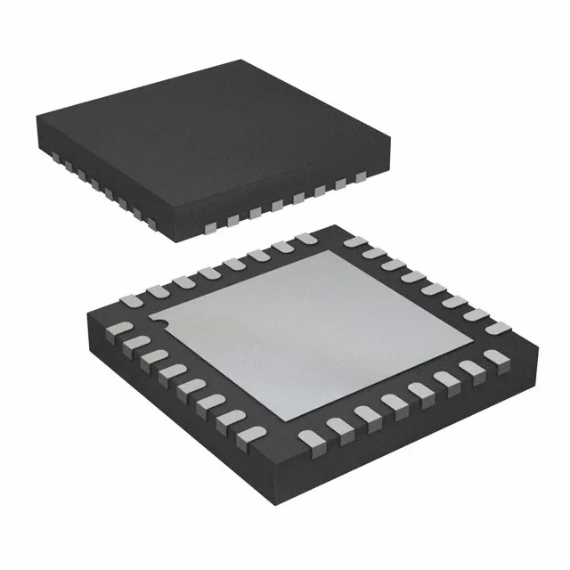
Analog Devices AD9552BCPZ — Clock & Timing ICs

AD9552BCPZ Clock Generator IC – 900 MHz, PLL, LVDS/LVPECL

MPNAD9552BCPZ
End of Life

Analog Devices AD9552BCPZ, Clock Generator, PLL Yes with Bypass, 900 MHz max frequency, CMOS/LVDS/LVPECL outputs, 32-LFCSP-WQ (5x5 mm), -40°C to 85°C operation.

$14.95Ref. price · indicative, final on quote
Packaging32-WFQFN Exposed Pad, CSP
StockContact for availability
MOQ1 pcs
  • 100% new & originalTraceable channels only — no refurbs, no pulls, no remarked parts.
  • Date & lot codes on quoteStated per line before you commit; label photos on request.
  • MSL-compliant ESD packingMoisture-sealed bags with indicator cards; reels photo-verified.
  • PayPal buyer protectionPay by T/T, PayPal or Payoneer — card payments covered end to end.

Specifications

AD9552BCPZ Technical Specifications
ParameterValue
TypeClock Generator
Mounting typeSurface Mount
Voltage3.135V ~ 3.465V
Frequency900MHz
Operating temperature-40°C ~ 85°C
PLLYes with Bypass
InputCMOS, Crystal
OutputCMOS, LVDS, LVPECL
PackageTray
Case32-WFQFN Exposed Pad, CSP
Divider (Multiplier)Yes/No
Number of circuits1
Ratio - Input:Output2:2
Differential - Input:OutputNo/Yes

Product details

900 MHz PLL clock generator with bypass

The AD9552BCPZ is a single-circuit clock generator from Analog Devices, integrating a PLL with a bypass option so you can switch between a clean on-chip synthesis path and an external reference clock without reconfiguring the board. It accepts CMOS or crystal inputs and delivers CMOS, LVDS, or LVPECL outputs up to 900 MHz, covering the common telecom and data-converter clock rates.

2:2 input-to-output ratio and differential output

With a 2:2 input-to-output ratio, the AD9552BCPZ accepts two single-ended references and produces two outputs — both can be configured as differential (LVDS or LVPECL) to drive long traces or high-speed ADCs. The PLL bypass path lets one output run as a clean buffer while the other remains PLL-locked, useful for clock-domain separation in mixed-signal systems.

Active production, 32-LFCSP package

The small footprint and 0.50 mm pitch require a well-planned thermal via array under the pad for heat sinking; the datasheet layout recommendation is worth following closely.

Frequently asked questions

Is the AD9552BCPZ compatible with 3.3 V logic?

The CMOS input thresholds track VDD, so a 3.3 V logic output drives the clock input without level shifting.

What is the closest functional second-source for the AD9552BCPZ?

The AD9552BCPZ-REEL7 is the same silicon in tape-and-reel packaging — electrically identical, just different reel format. For a higher-frequency sibling with more outputs, the AD9522-5BCPZ runs to 2.4 GHz and offers 12 or 24 outputs, but it requires a differential input and has a larger package.