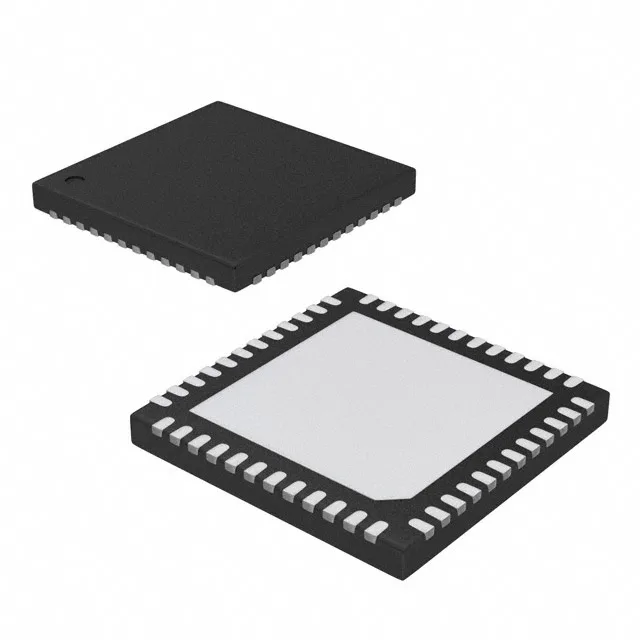
2.95 GHz PLL clock generator with 12-output fanout
The AD9517-0ABCPZ integrates a PLL with an on-chip VCO to generate clock signals up to 2.95 GHz, then distributes them across 12 differential LVDS or LVPECL outputs in a single 48-LFCSP package. That 1:12 fanout ratio means one device can clock an entire multi-channel ADC or FPGA transceiver bank without external fanout buffers — saving board space and reducing jitter accumulation from cascaded dividers.
The supply rail is 3.135V to 3.465V — a tight 3.3V ±5% window — so the board needs a clean regulated rail; a switching regulator feeding this part should have a post-LDO or at least a low-noise LDO to keep the PLL in lock and the output jitter within spec.
Analog Devices lists the AD9517-0ABCPZ as Active. The part is ROHS3 compliant.
Input flexibility and output configuration
The reference input accepts CMOS, LVDS, or LVPECL levels, so it can lock to a crystal oscillator, a TCXO, or a backplane clock without level translation. The 12 outputs are all differential — LVDS or LVPECL — which means each output pair drives a 100-Ω terminated line with good noise immunity. The divider/multiplier block (Yes/No) lets you generate sub-harmonics of the VCO frequency, but there is no on-chip multiplier for the PLL feedback path.