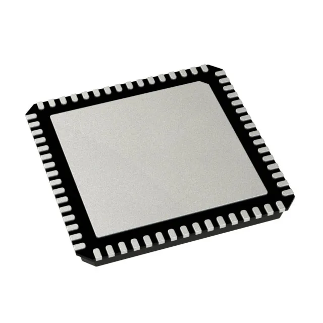
Analog Devices AD9516-1BCPZ-REEL7 — Clock & Timing ICs

AD9516-1BCPZ-REEL7 Clock Generator, 2.95 GHz, Active

MPNAD9516-1BCPZ-REEL7
End of Life

Analog Devices AD9516-1BCPZ-REEL7, Clock Generator, Fanout Distribution, PLL Yes, 1:14 input:output ratio, 2.95 GHz max frequency, CMOS/LVDS/LVPECL outputs, 64-VFQFN Exposed Pad (64-LFCSP-VQ 9x9), -40°C to 85°C, ROHS3 compliant.

$19.71Ref. price · indicative, final on quote
Packaging64-VFQFN Exposed Pad, CSP
StockContact for availability
MOQ1 pcs
  • 100% new & originalTraceable channels only — no refurbs, no pulls, no remarked parts.
  • Date & lot codes on quoteStated per line before you commit; label photos on request.
  • MSL-compliant ESD packingMoisture-sealed bags with indicator cards; reels photo-verified.
  • PayPal buyer protectionPay by T/T, PayPal or Payoneer — card payments covered end to end.

Specifications

AD9516-1BCPZ-REEL7 Technical Specifications
ParameterValue
TypeClock Generator, Fanout Distribution
Mounting typeSurface Mount
Voltage3.135V ~ 3.465V
Frequency2.95GHz
Operating temperature-40°C ~ 85°C
PLLYes
InputClock
OutputCMOS, LVDS, LVPECL
PackageTape & Reel (TR); Cut Tape (CT)
Case64-VFQFN Exposed Pad, CSP
Divider (Multiplier)Yes/No
Number of circuits1
Ratio - Input:Output1:14
Differential - Input:OutputYes/Yes

Product details

What this clock generator does for your clock tree

The AD9516-1BCPZ-REEL7 is a clock generator and fanout distribution IC from Analog Devices, integrating a PLL to synthesize and distribute up to 14 clock outputs from a single input. It supports CMOS, LVDS, and LVPECL output formats, letting you drive mixed-logic clock trees without external level translators. Its 2.95 GHz maximum frequency targets high-speed ADC/DAC clocking, FPGA reference clocks, and RF LO distribution where jitter and skew matter. The 1:14 fanout ratio reduces the number of clock buffers and splitters on the board, simplifying layout and saving space.

Why the 2.95 GHz ceiling matters for your design

At 2.95 GHz, this part covers L-band and lower C-band applications, including cellular base station local oscillators, radar IF sampling clocks, and high-speed data converter clocking. The PLL with integrated VCO means you get a complete synthesis loop in one package — no external VCO or loop-filter design needed. The differential input and output capability preserves signal integrity over long PCB traces and through connectors, critical when routing clocks across a multi-card backplane or to remote ADC banks.

It is ROHS3 compliant, meeting current environmental regulations for solder reflow and end-product compliance.

Package and supply rail checklist

Surface-mount 64-VFQFN exposed pad, also specified as 64-LFCSP-VQ (9x9). The 3.135V to 3.465V supply range is a tight 3.3V nominal ±5% — a clean 3.3V rail with low ripple is essential for PLL phase-noise performance. Plan for dedicated LDO or filter on the supply input.

Frequently asked questions

What is the maximum frequency of the AD9516-1BCPZ-REEL7?

The maximum output frequency is 2.95 GHz, making it suitable for L-band and lower C-band clock generation and distribution in RF and high-speed data converter applications.

What are the closest functional equivalents to the AD9516-1BCPZ-REEL7?

The AD9516-0BCPZ-REEL7 and AD9516-4BCPZ share the same PLL, output types (CMOS, LVDS, LVPECL), 2.95 GHz max frequency, 1:14 ratio, and 64-LFCSP package. The AD9518-1ABCPZ-RL7 is a 2.65 GHz variant with only 6 outputs and LVPECL outputs. Confirm the exact output count and frequency requirement before substituting.

What package type does the AD9516-1BCPZ-REEL7 use?

It is supplied in a 64-VFQFN exposed pad package, also designated as 64-LFCSP-VQ (9x9).