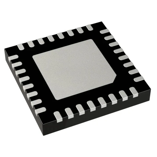
What this clock buffer does for a 1.6 GHz clock tree
The AD9515BCPZ-REEL7 is a 1:2 fanout buffer with an integrated divider, rated to 1.6 GHz maximum input frequency. It accepts a single clock input and delivers two outputs, each independently selectable as CMOS, LVDS, or LVPECL levels. The divider stage lets you generate a sub-rate clock from a higher-frequency reference — useful when the FPGA or ADC needs a lower-speed sample clock derived from the same oscillator that drives the system PLL.
The supply range is 3.135V to 3.465V — a tight 3.3V ±5 % window. A noisy rail couples into the output jitter; plan a dedicated low-noise LDO for this rail, not a shared switcher.
It is ROHS3 compliant. The base part AD9515BCPZ is the same silicon in a different shipping format — the two are electrically identical and interchangeable on the board.
How it compares to the AD9514 and AD9512 siblings
The AD9514BCPZ-REEL7 is the closest functional sibling: same 1.6 GHz ceiling, same output types, but a 1:3 fanout ratio instead of 1:2. If your BOM needs three clock fanouts from one input, the AD9514 saves a second buffer IC. The AD9512 and AD9511 run at 1.2 GHz max and offer a 2:5 fanout with two input muxes — they suit lower-speed clock trees that need more distribution legs. The AD9515 is the right pick when the reference clock runs above 1.2 GHz and only two outputs are needed.