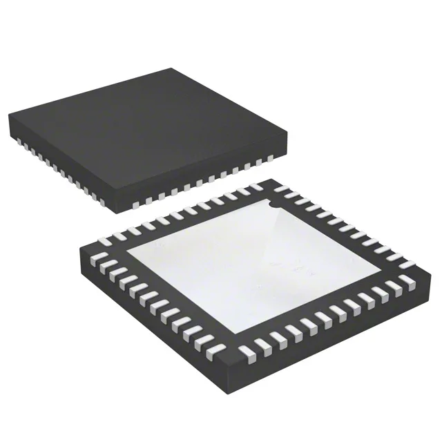
Analog Devices AD9512BCPZ — Clock & Timing ICs

AD9512BCPZ Clock Buffer 2:5 1.2 GHz LFCSP

MPNAD9512BCPZ
End of Life

Analog Devices AD9512BCPZ, Fanout Buffer (Distribution), Divider, 2:5 input:output ratio, 1.2 GHz max frequency, CMOS/LVDS/LVPECL outputs, 48-LFCSP-7x7, -40°C to 85°C.

$19.03Ref. price · indicative, final on quote
Packaging48-VFQFN Exposed Pad, CSP
StockContact for availability
MOQ1 pcs
  • 100% new & originalTraceable channels only — no refurbs, no pulls, no remarked parts.
  • Date & lot codes on quoteStated per line before you commit; label photos on request.
  • MSL-compliant ESD packingMoisture-sealed bags with indicator cards; reels photo-verified.
  • PayPal buyer protectionPay by T/T, PayPal or Payoneer — card payments covered end to end.

Specifications

AD9512BCPZ Technical Specifications
ParameterValue
TypeFanout Buffer (Distribution), Divider
Mounting typeSurface Mount
Voltage3.135V ~ 3.465V
Frequency1.2 GHz
Operating temperature-40°C ~ 85°C
InputClock
OutputCMOS, LVDS, LVPECL
PackageTray
Case48-VFQFN Exposed Pad, CSP
Number of circuits1
Ratio - Input:Output2:5
Differential - Input:OutputYes/Yes

Product details

1.2 GHz fanout buffer with three output standards

The AD9512BCPZ is a clock fanout buffer and divider from Analog Devices, rated for a maximum input frequency of 1.2 GHz. It accepts two clock inputs and distributes them to five outputs, each independently programmable to CMOS, LVDS, or LVPECL levels. The 2:5 fanout ratio means a single reference clock can feed five downstream devices — an ADC, an FPGA, a SerDes, a DAC, and a monitor port — all from one buffer, saving board space and reducing clock-tree jitter from multiple discrete fanout gates.

Output flexibility — CMOS, LVDS, LVPECL per channel

Each of the five outputs can be set to CMOS, LVDS, or LVPECL independently, so a mixed-signal board with a CMOS FPGA input, an LVDS ADC clock, and an LVPECL SerDes reference can all be driven from the same buffer without external translators. The input and output paths are fully differential, which gives better common-mode noise rejection than single-ended clock distribution — important when routing clocks across a noisy mixed-signal board.

Package and footprint — 48-LFCSP with exposed pad

Housed in a 48-lead LFCSP (7x7 mm) with an exposed pad, the package requires a thermal land on the PCB to pull heat from the die. Surface-mount only — the LFCSP demands a controlled solder-paste stencil and a reflow profile that matches the package's moisture sensitivity level.

Frequently asked questions

Where can I buy AD9512BCPZ in stock?

Sourcing buyers need immediate inventory and lead time to fill BOM lines without delay.

What is the AD9512BCPZ datasheet and specifications?

Design engineers validate fit by checking electrical characteristics, pinout, and timing diagrams.

What is the price for AD9512BCPZ?

Buyers compare pricing across distributors to optimize procurement cost.

Is AD9512BCPZ equivalent to any other clock buffer?

Maintenance techs and brokers need cross references for replacement or obsolete part identification.

What is the pinout of AD9512BCPZ?

Engineers need pin mapping for PCB layout and to ensure compatibility with existing designs.

What is the lead time for AD9512BCPZ?

Production planners need accurate lead times to avoid manufacturing delays.