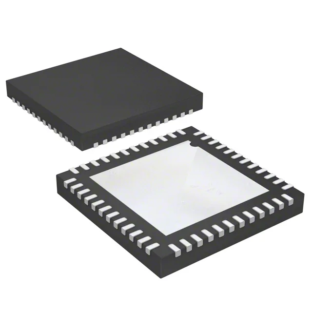
The AD9511BCPZ is a 2:5 fanout buffer and clock divider from Analog Devices, rated for a maximum input frequency of 1.2 GHz. That ceiling covers the reference clocks for most high-speed ADCs, DACs, and FPGA transceivers — the part does not limit the system clock rate below the converter's own maximum. The 2:5 input-to-output ratio means two independent clock sources can be selected and distributed to five outputs. In a base station or radar receiver, one input carries the main system clock and the second a backup reference; the buffer switches without an external mux. Outputs are configurable as CMOS, LVDS, or LVPECL, and the part accepts differential inputs and delivers differential outputs. For a layout engineer, this means the clock tree can stay fully differential from source to load, preserving signal integrity across a backplane or long PCB trace.
Supply rail and temperature — industrial-grade timing
A switching regulator feeding this rail needs output ripple below 10 mV to avoid injecting jitter into the clock path; an LDO post-regulator is the safer choice for phase-noise-sensitive designs. This qualifies the part for outdoor telecom cabinets, engine-bay electronics, and factory-floor equipment where ambient temperature swings exceed commercial limits.
Package and footprint — 48-LFCSP with exposed pad
The AD9511BCPZ is supplied in a 48-lead LFCSP-VQ package measuring 7 mm × 7 mm, with an exposed pad. The package is supplied in a tray, not tape-and-reel.
The part is ROHS3 compliant. The part is sourced through our distribution network — submit an RFQ for a firm price and lead-time commitment.