Its 40 MHz gain-bandwidth product and 300 V/µs slew rate place it in the high-speed general-purpose class, suited for signal conditioning, active filters, and buffer stages where the board environment is commercial temperature (0°C to 70°C) and the supply rails can span 10 V to 36 V.
The 300 V/µs slew rate and 40 MHz GBW together define the large-signal and small-signal speed boundaries. For a 10 V output swing, the slew rate limits full-power bandwidth to roughly 4.8 MHz — beyond that, the output distorts into a triangle wave. The 40 MHz GBW means closed-loop gain of 10 gives a usable 4 MHz small-signal bandwidth. These numbers matter when the op-amp drives a fast ADC input or reconstructs a waveform from a DAC: the 300 V/µs rate keeps the output from slewing on sharp edges, preserving the signal's shape.
Package and mounting — the through-hole reality
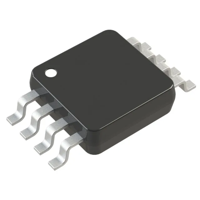
The AD841JH comes in a TO-8 style metal can with 12 leads (TO-8-12). It is a through-hole mount part, which means the leads insert into plated holes on the PCB and are soldered on the opposite side. This form factor is common in legacy instrumentation, avionics retrofit boards, and prototyping where socketing is preferred.
The supply span runs from 10 V minimum to 36 V maximum, giving flexibility for ±5 V to ±18 V split supplies or a single 12 V to 24 V rail. Quiescent current is 11 mA, which is moderate for a 40 MHz amplifier — not a low-power part, but reasonable for its speed class. Each channel can deliver 50 mA of output current, enough to drive a 50 Ω load to ±2.5 V or a 100 Ω load to ±5 V, making it suitable for line drivers and coaxial cable interfaces in test equipment.
Input offset and bias current — the DC precision trade-off
Input offset voltage is 800 µV maximum, and input bias current is 3.5 µA. The bias current is high by modern standards — a bipolar input stage — which means source impedance must be kept low to avoid offset voltage errors from the bias current flowing through the source resistance. For a 1 kΩ source, the 3.5 µA bias adds 3.5 mV of offset; for a 10 kΩ source, it adds 35 mV. This part is not the choice for high-impedance sensor interfaces, but it works well with low-impedance sources like op-amp outputs, DACs, and terminated transmission lines.
Note that it is listed as RoHS non-compliant, which is expected for a hermetic metal-can package from this era — the part contains lead in the solder seal and lead finish. For new designs requiring RoHS compliance, a tin-plated or Pb-free equivalent would need to be sourced; for repair and legacy production, the non-compliant status is typically accepted under exemption.