Its 50 ns max propagation delay means it can resolve a 20 MHz input transition and still leave timing margin for the downstream logic — useful in zero-crossing detectors, overcurrent trip circuits, and high-speed ADC front ends where the comparator's decision must settle before the next clock edge. The built-in latch holds the output state after the strobe, so a microcontroller can read the result at its own pace without missing a fast event.
Supply range and output compatibility
The output swings to CMOS and TTL levels, so it drives a 5 V logic input directly and, with a resistive divider, can feed a 3.3 V GPIO without a level translator — one less BOM line. Input offset voltage maxes at 1.5 mV at 5 V, and the 500 µV of hysteresis cleans up chatter on slow-moving signals, which saves adding external positive feedback resistors.
Through-hole package — breadboard and retrofit fit
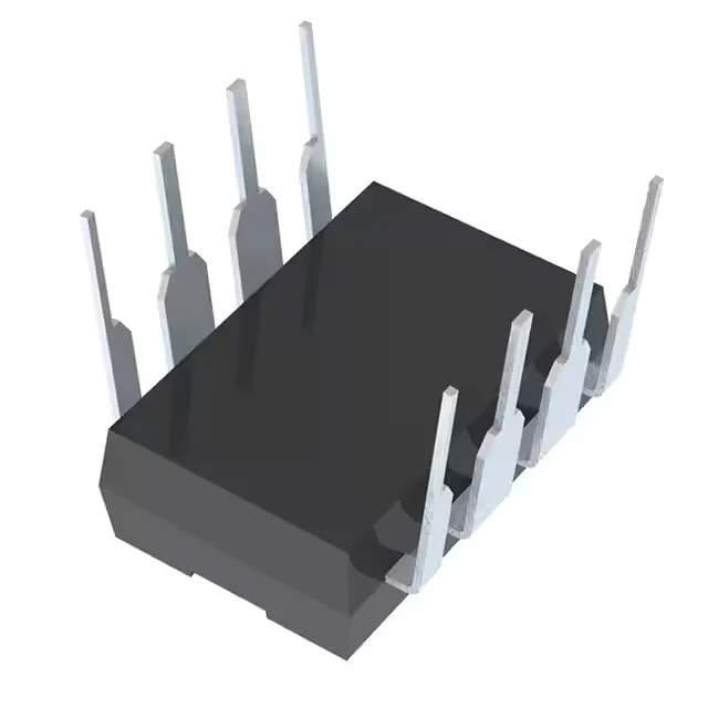
Housed in an 8-DIP (0.300", 7.62 mm) through-hole package, the AD790JNZ is a natural fit for breadboard prototyping, socketed test fixtures, and legacy boards that avoid SMT. The 8-PDIP supplier device package is a standard footprint with 0.100" pin spacing, so it drops into existing sockets without a layout change. Quiescent current maxes at 10 mA, and input bias current stays under 5 µA at 5 V — both moderate figures that suit benchtop and industrial control applications where power is not the tightest constraint.
For dual-sourcing flexibility, the surface-mount sibling AD790JRZ shares the same 50 ns speed, 500 µV hysteresis, and CMOS/TTL output but in an SOIC package — useful if a board spin moves to SMT. The AD790JNZ is RoHS3 compliant.